Contract development
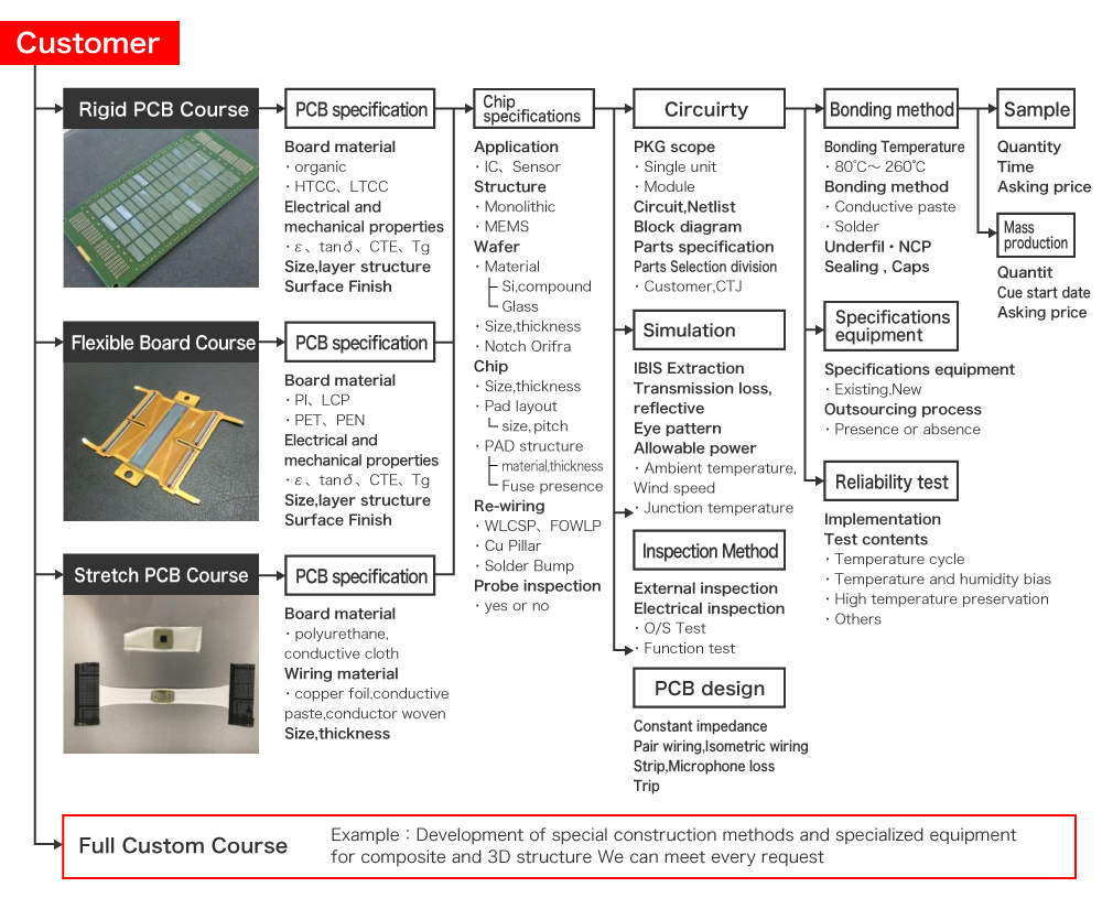
Development and Support
We will support prototyping, evaluation, failure analysis and mass production, comprehensively.
By connecting all technologies of the Japan, which is the origin of our company name, not only semiconductor packages, We provide comprehensive support for the semiconductor chip, MEMS Chip, PCB assembly, module, prototype, evaluation, analysis, reliability evaluation, and mass production. We provide services to meet the needs of our customers through cooperation with affiliated companies, research institutes, universities, etc.
OSRDA corresponding example
Environmental Reliability Test Development
Why Choose Us
Supporting wide areas of business domain
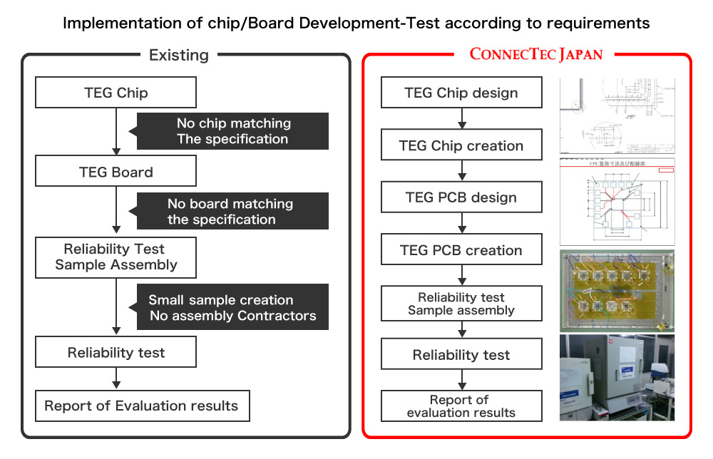
We will provide total solutions with clients from device and substrate design, proto-typing, reliability test to mass-production. We also provide clients with highly value added services in cooperation with our partner companies and research institutions all over the world.
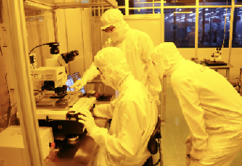
Corresponding to various kinds and/or types of chip assembly
IoT and wearable applications, and to meet the diversification of 5G implementation of high-speed and functional devices. Low-load damage-free mounting to the any type of substrate. In addition, by the newly developed desktop type of equipment, the multi-product variable production can be arranged.
Quick turn-around-time
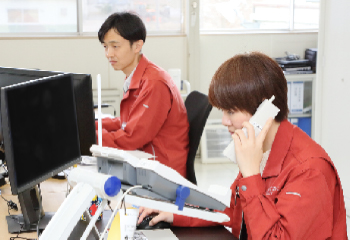
We respond to inquiries, provide quotation, implement structure and process proposals, and prototypes quickly without having to wait. In the case of a standard process, we quote in 2 working days and prototype is available in two to six weeks.
Development Contract Service Flow
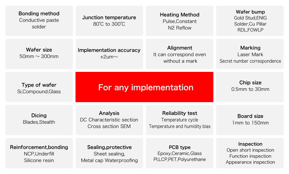
In order to meet any demands of our customers, Connectec Japan has prepared a development, prototyping, and analysis environment against a wide variety of semiconductor packaging requirements. We can handle with variety of semiconductors, MEMS, etc. In Head office R&D center, we have wafer dicing, printing, flip-chip bonding, laser marking, and even non-in-house processes, we can connect the Japan nationwide partner companies to develop and prototype.
Research and development and prototyping environment
We have assembling equipment such as wafer dicing, printing, flip chip bonding, X-ray transmission inspection system, electron microscope/Energy dispersive X-ray spectrometer(SEM/EDX), evaluation and analysis equipment such as temperature cycle. In addition, it is possible to respond to all requests through cooperation with partner companies nationwide Japan.
Trial process Menu
In order to meet all customer’s requirement, we can process various substrates such as ceramics, organic, film, etc., depending on the bonding form of semiconductor chips and modules. We have prepared MonsterPAC process . This process menu proposes the best process and implementation structure to meet your requirements.
