Contract development
MONSTER PAC® Core Technology
Bump On Material and Damage Free Bonding
Our MONSTER PAC® is the world’s first and original cutting-edge technology.
Strength
Bump On Material
Bumps are formed on the materials.Conjunctions are performed by conductive paste.
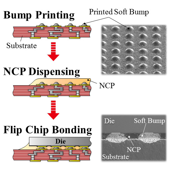
Bump On Wafer
Bonding takes place with low temp.low load. Strong and sufficient adhesion. Our low temp.low load ‘damage free’ bonding is the only answer to the fragile 5G requirement.
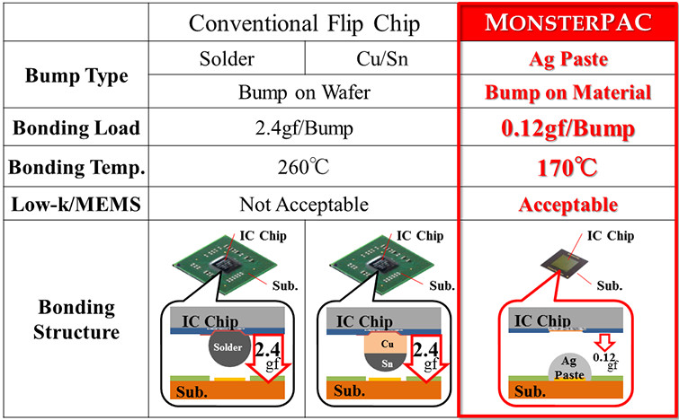
Feature
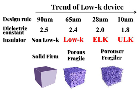
high speed, more functions requirement for LSI, circuit design rule is getting finner and narrower. To control capacity between layers as low to meet high speed, insulator between layers is getting more porous and weaker against mechanical damage. CONNECTEC JAPAN’s MONSTER PAC® ‘damage free’ bonding can process such ‘Low-k’ insulation layers without damage while conventional bonding cannot process ‘Low-K’ device without damage.
solid and movable configuration
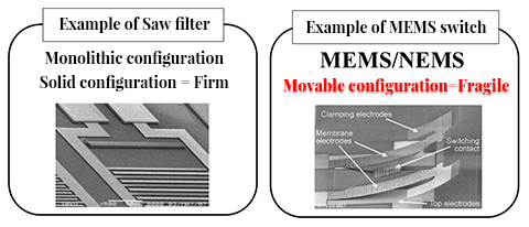
conventional process cannot assemble fragile MEMS/NEMS due to possible physical damage. Left sketch shows SAW filter with monolistic configuration. Right sketch shows solid configuration MEMS device and conventional process can build the device. However, conventional process cannot build MEMS device with movable configuration due to fragility.
Low-k device trend
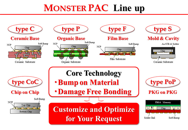
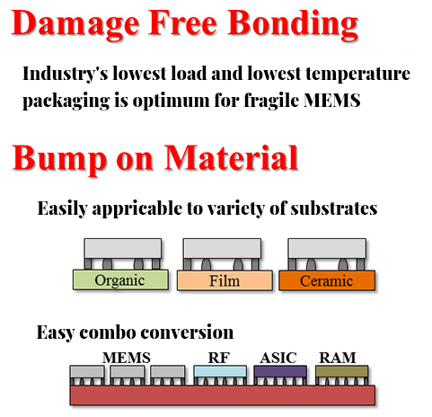
MONSTER PAC® – damage free bonding, low temp./low load, core technology of CONNECTEC JAPAN enable sensitive MEMS/NEMS assembly. And to meet high functionality requirement, combo of MEMS device and LSI become more popular. MONSTER PAC® is applicable to variety of substrates, i.e. organic, tape, ceramic, and form bumps on substrate side which is easier to make combos with LSI, RF, and other chips.
Based on various customers’ requirement, we have standard packages line-up. For further details, please contact CONNECTEC JAPAN.
